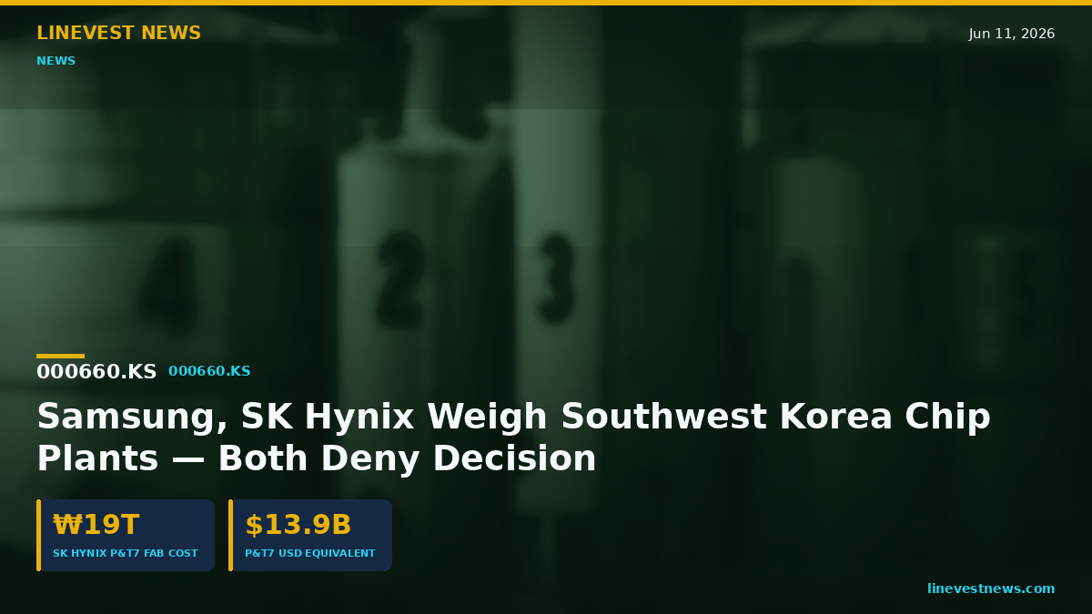
A wave of reports that Samsung Electronics (005930.KS), the world's largest memory-chip maker, and SK Hynix (000660.KS), the world's top supplier of high-bandwidth memory (HBM), are weighing major semiconductor investments outside the Seoul metropolitan area has set off a scramble among provincial governments. Both companies, however, say nothing has been decided — leaving the central question for an investor unanswered: is there real, sized capital expenditure here, or political momentum running ahead of any board decision?
What is actually confirmed versus rumored
The firmest data point belongs to SK Hynix, and it predates the current speculation. The company broke ground in April on its P&T7 advanced packaging fab in Cheongju, North Chungcheong Province, a roughly ₩19 trillion (USD13.9 billion) project (per The Elec; Korea Herald). Advanced packaging — the back-end step that stacks and bonds finished dies — has become central to HBM, the memory used in AI accelerators, which is why both chipmakers are expanding it.
Beyond that, the reports are unconfirmed. Samsung has been reviewing, since earlier this year, a chip packaging (back-end) facility in Gwangju, Korea's largest southwestern city in the Honam region (Korea Herald; The Elec). SK Hynix is named as a possible investor in further back-end capacity outside the capital region, though any additional spend is seen as more likely to cluster in Chungcheong, where it already runs Cheongju (Korea Herald).
Crucially, both companies pushed back. They "declined to comment directly on the reports, saying they were unaware of the matter," with messaging that "nothing has been decided on regional investment" (The Elec; Korea Herald).
Why the political pressure is building now
The speculation has gained force because the administration of President Lee Jae Myung is pressing large conglomerates to invest beyond Seoul to support balanced regional growth (Korea Herald). The two chipmakers are reportedly coordinating with the government over whether to unveil any regional plans at a presidential roundtable scheduled for later in June (The Elec) — the single event most likely to convert rumor into a confirmed number.
Local officials are not waiting. Jeonnam Province (South Jeolla) on June 11 urged Samsung and SK Hynix to build a fab and advanced-packaging complex in the Jeonnam–Gwangju area, calling for a "Honam semiconductor cluster" (Yonhap). Politicians in Sejong and South Chungcheong have made competing pitches for the same investment (Yonhap).
The historical frame
The scale of what a Gwangju plant would represent is best measured against Samsung's own history: its last domestic back-end base was the Onyang campus established in 1991 — making a new packaging site its first in roughly 35 years (Korea Herald). For now, SK Group Chairman Chey Tae-won has signaled the priority lies elsewhere, telling reporters on the sidelines of a forum in Japan on June 10 that "the most important thing is to build Yongin properly. But demand is growing so rapidly that our plans have clearly moved faster" (Korea Herald), referring to the chipmakers' flagship cluster south of Seoul.
The rationale driving the search is structural — land and power constraints are tightening in the Seoul-area chip belt, pushing the next generation of capacity outward (Korea Herald; The Elec).
The data point to watch
The presidential roundtable later in June is the confirming or refuting signal. If either company attaches a region, a won figure and a timeline there, the provincial competition becomes a real capex story; if not, the denials stand and the headlines remain political positioning. Samsung operates packaging lines in Onyang and Cheonan in South Chungcheong today (Korea Herald), so a southwestern site would mark a genuine geographic break rather than an extension of existing back-end footprint.
This article is for informational purposes only and does not constitute investment advice. Figures are sourced from the outlets cited inline; the ₩/USD conversion uses an approximate rate of 1,370 won per dollar.