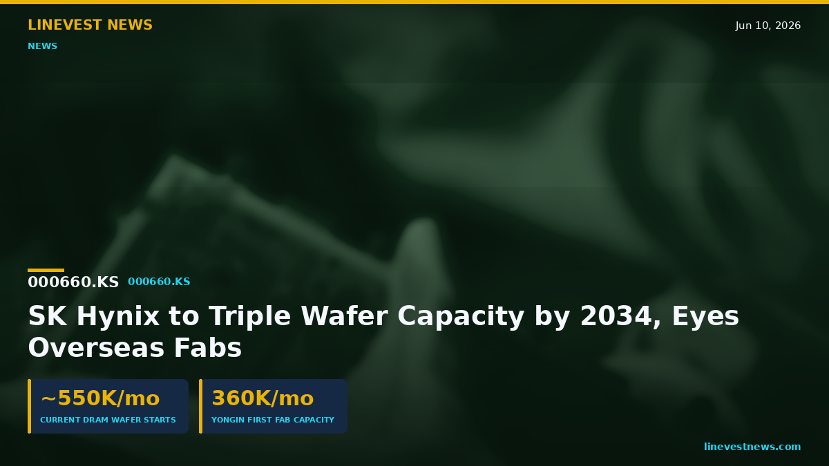
SK Hynix (000660.KS), Korea's second-largest chipmaker by revenue and the world's leading supplier of high-bandwidth memory (HBM) used in AI servers, will triple its wafer fabrication capacity by 2034 to meet demand for AI memory, SK Group Chairman Chey Tae-won told Nikkei Asia in an interview published June 10. In the same round of comments in Tokyo, Chey signaled the company's next fabs may not all be built in Korea — the detail most likely to unsettle assumptions about where the buildout actually lands.
How big is "triple" in wafer terms?
In absolute terms, the trajectory is steep. SK Hynix runs roughly 550,000 monthly DRAM wafer starts today and has been briefing equipment and materials suppliers on a plan to reach about 1 million wafers per month by 2030–2031, according to TechTimes (June 6) — a near-doubling that precedes the 2034 tripling target. Chey separately framed the nearer milestone as doubling capacity "within five years" and said the company is moving "at full speed," per The Elec. He cautioned that a new fab "takes at least three years, and more than five years when starting from scratch," and that SK Hynix does not work from a predetermined spending figure but invests as costs rise (The Elec).
Why "overseas" is on the table
Speaking to reporters after the Nikkei Forum's Korea-Japan session at Tokyo's Imperial Hotel, Chey said the location for the next plant would be decided "comprehensively," weighing land, electricity, water and workforce. "If it can't be done in Korea, there may be situations where we have to build overseas... it won't necessarily be Korea only," he said, per ET News and Chosun Biz. Nikkei reported that Japan is viewed as an "excellent candidate" for an overseas site. Chey stressed that the immediate priority remains the domestic Yongin cluster.
That cluster — under construction across about 4.16 million square meters in Yongin, a city south of Seoul — will house four fabs, per Chosun Biz. The first fab alone is designed to add 360,000 wafers per month at full capacity by the first half of 2030, built across six cleanrooms of 60,000 wafer starts each, with equipment move-in for the first cleanroom pulled forward to February 2027 from an earlier May 2027 target (TechTimes). The M15X fab in Cheongju is set to start in the second half of 2026 at 40,000 wafers per month, rising toward 80,000 in 2027 (TechTimes).
The demand the whole plan rides on
The expansion lands amid what one Chosun Biz analysis called a "semiconductor mirage." Korea's May exports hit a record $87.75 billion (up 53.2% year-on-year), of which semiconductors made up 42.3% — versus roughly 10% during the 1990s chip boom. The cautionary precedent: after the 1995 memory peak, DRAM prices fell 51% and 65% in 1996 and 1997, a downturn economists count among the triggers of Korea's 1997 foreign-exchange crisis (Chosun Biz). The OECD now projects Korea's potential growth to fall below 1.5% next year for the first time, the same analysis noted. Chey himself ties the buildout to a memory shortage he expects to persist through 2030 (The Elec) — making the durability of that shortage the single variable the capacity plan depends on.
The capacity message coincided with deeper Korea-Japan tech alignment. On June 10, SK Telecom (017670.KS), Korea's largest mobile carrier, joined Japan's NTT — the country's largest telecom group — and Taiwan's Chunghwa Telecom to launch a $500 million (₩760 billion) "IOWN" AI fund through a new vehicle, Catalight Capital, targeting AI data-center, chip and optical-networking startups; SK Hynix is preparing to participate, per Chosun Biz.
What confirms or refutes it next
The next concrete signal comes June 29, when Samsung and SK are due to disclose regional investment plans at a meeting at the Blue House (Korea's presidential office) chaired by President Lee Jae-myung, with politicians pressing for new fabs in the Honam and Chungcheong regions (Chosun Biz) — a domestic test of Chey's "not necessarily Korea only" hedge.
This article is for informational purposes only and does not constitute investment advice. Figures are sourced from the outlets cited inline and were accurate as of publication.
Sources
- https://asia.nikkei.com/business/tech/semiconductors/sk-hynix-to-triple-wafer-capacity-by-2034-chairman-chey
- https://www.thelec.net/news/articleView.html?idxno=10992
- https://www.techtimes.com/articles/317859/20260606/sk-hynix-dram-capacity-roadmap-revealed-yongin-alone-adds-360k-wafers-monthly.htm
- https://biz.chosun.com/industry/company/2026/06/10/VRNQZ2UIDVB2HJGHOVPRH6MY2A/
- https://www.etnews.com/20260610000459