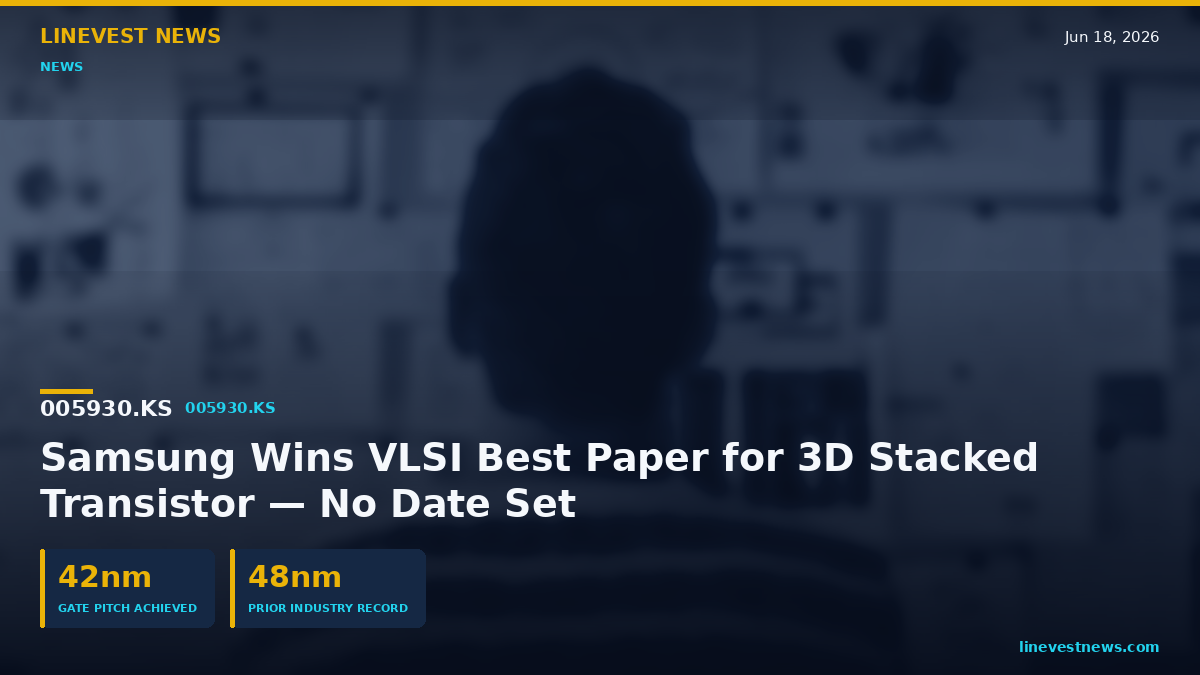
Samsung Electronics (005930.KS), the world's largest memory-chip maker and South Korea's most valuable listed company, said its Logic TD Team at the Semiconductor R&D Center built a 3D stacked transistor that it says reaches an industry-first 42-nanometer gate pitch and took the Best Paper award at the 2026 Symposium on VLSI Technology and Circuits in Hawaii, held June 14-18, per Seoul Economic Daily's English edition (en.sedaily.com). For a portfolio manager, the headline raises one question: is this a lab result, or a manufacturing lead that helps Samsung's foundry business close the gap with Taiwan's TSMC — and when would it touch revenue? On the evidence Samsung disclosed, it is the former, with the second part still unanswered.
What was actually demonstrated
The device is a 3D Stacked Field-Effect Transistor (3D Stacked FET) — instead of placing n-type and p-type transistors side by side on a flat plane, Samsung stacked them vertically. The company reported a gate pitch of 42 nanometers, down from the previous industry record of 48nm, which it describes as the smallest yet for this architecture (en.sedaily.com; The Asia Business Daily, asiae.co.kr). It stacked three nanosheet channel tiers on both the upper and lower transistors — more than the two used previously — and says the result roughly doubles transistor density, equivalent to about a 50% reduction in area on the same wafer (asiae.co.kr).
To size the claim: Samsung frames the design as offering up to a theoretical 100% performance gain, against the roughly 15% improvement a conventional process node delivers per generation (asiae.co.kr), alongside a claimed twofold power-efficiency gain. The paper was selected as Best Paper from more than 1,000 submissions, according to both outlets. A key engineering step was an I-shaped, straight-down through-connection linking the stacked tiers, replacing U-shaped side connections. "42 nm is the world's smallest size, implemented for the first time in the industry," said Kwon Wook-hyun, one of the paper's authors on Samsung's Logic TD Team (en.sedaily.com).
Why a fund manager should read it carefully
The relevant comparison is 2022, when Samsung became the first chipmaker to mass-produce a 3nm node using Gate-All-Around (GAA) MBCFET transistors, ahead of TSMC, which planned to adopt GAA only at its 2nm node (Samsung Global Newsroom, news.samsung.com). That milestone showed Samsung can hit a process-technology first — but it did not translate into the foundry market-share gains against TSMC that the technical lead implied, illustrating the distance between a conference trophy and customer wins.
The same caveat applies here. A 3D Stacked FET, like complementary-FET designs across the industry, is a forward-looking architecture; Samsung announced no mass-production timeline and no process node for the technology. The performance and density figures are described as theoretical. So the result confirms Samsung's R&D is at the frontier of vertical scaling, but it is not yet a shipping product or a booked foundry order.
The data point that would confirm it
The item to watch is not the paper but the roadmap: whether Samsung folds 3D stacking into a named foundry node and announces external customers. Updates typically surface at Samsung Foundry Forum events and in quarterly results commentary. Until a node and a timeline appear, the achievement sits in the research column. (Separately, the same news cluster carried consumer items the same week, including the domestic launch of the budget Galaxy A37 5G at ₩598,400, about USD 431 — etnews.com — financially immaterial next to the foundry question.)
This article is for informational purposes only and does not constitute investment advice. Figures are sourced as cited and reflect company claims, several of which Samsung describes as theoretical.